A brief history of Computers
The precursor of modern computers - the Analytical Engine - was proposed by Charles Babbage in the 1800s. Although it was never fully built, this is the first mechanical general-purpose computer, powered by steam, that featured a CPU-like processor, memory, and programmable input devices such as punched cards. This design laid the groundwork for concepts in general-purpose computing, including the separation of processing and storage. Around the same time, Ada Lovelace is the first to recognize that the Analytical Engine has applications beyond pure calculation, and is often recognized as the first computer programmer. During that time, a computer wouldn’t even need power to run, as it was just a huge mechanical engine with the core components of computers.
Computers began to use electrical power in the 1940s. ENIAC is one of the first electronic computers completed at the University of Pennsylvania for the US Army. It famously used 18000 vacuum tubes that act as electronic switches to represent 0s and 1s for calculation. However, vacuum tubes are large and fragile. Subsequantly in the 1950s, transistors were used to replace vacuum tubes. It is smaller, cooler, and performs the same switching function. In the 1960s, engineers packed many transistors onto a single piece of silicon, which we called an integrated circuit, making electronics cheaper and more compact. In 1971, Intel first introduced its microprocessor, the Intel 4004, which means that they placed an entire central processing unit on one chip. This miniaturization is what eventually made personal computers practical and affordable.
After the microprocessor was born, personal laptops and workstations emerged in the 1980s. From the 1980s to 2004, Dennard scaling showed that more transistors could be packed on the same chip without increasing total heat, because power density remained constant as voltage and current scaled down. This has enabled faster speed of computing and lower power per task. However, this scaling broke down in 2004 because the current and voltage couldn’t keep dropping. This observation has helped companies such as Intel shift from single-core to multicore processors.
Power and Energy in Integrated Circuits
At a high level, power has two needs. Firstly, power must be brought in and distributed around the chip. Modern microprocessors use hundreds of pins and multiple interconnect layers just for power and ground. Secondly, power is dissipated as heat and must be removed from the chip.
As engineers, when we think about power, there are two things we need to consider. First, think about the maximum power a processor ever requires. This will help you to decide how much current the processor ever needs to draw from a power supply system. Second, consider the sustained power consumption, or, in industry terms, the thermal design power (TDP), as this is needed to determine your cooling requirements. TDP is neither the peak power, which is often 1.5 times higher, nor the actual average power consumed during a given computation, which is likely to be lower still. A system is usually aimed for a power supply above TDP, and a cooling system is designed to match the TDP. Failure to provide adequate cooling will allow the junction temperature in the processor (where the transistors are) to exceed its maximum value, resulting in device failure and possibly permanent damage.
Modern processors provide two extra features to manage heat. Firstly, as the thermal temperature approaches the junction temperature limit, the processor lowers the clock rate, thereby reducing power and heat generation. If the first attempts to reach the target temperature fail, a second thermal overload trap (emergency shutdown) is activated to power down the chip.
CMOS
CMOS, Complementary metal-oxide semiconductor, is a type of metal–oxide–semiconductor field-effect transistor (MOSFET) fabrication process that uses complementary and symmetrical pairs of p-type and n-type MOSFETs for logic functions.
 Source: Image extracted from [3]
Pure silicon is a poor conductor with 4 valence electrons and forms a stable crystal lattice. N-type means that the silicon is doped with elements with 5 valence electrons (eg, phosphorus), thus the extra electron is free to move, and creates mobile negative charges. P-type means that the silicon is doped with elements with 3 valence electrons (eg, boron). This creates a positive charge as it has a missing electron. When N-type and P-type meet, they create a PN junction that allows electrons to flow in one direction.
Materials
The primary material used in CMOS is silicon (Si), derived from silicon dioxide (sand). Silicon serves as the semiconductor substrate upon which transistors are built. Other key materials include Silicon dioxide, which is traditionally used as a gate insulator, copper for interconnect wires, etc.
Transistors
Below shows an example of a CMOS inverter, which is a NOT gate.
Source: Image extracted from [5]
![]() Source: Image extracted from [4]
Source: Image extracted from [4]
When the input is 1:
- High voltage applies to both gates.
- NMOS is ON. The positive gate voltage attracts the electrons to the surface of the P-substrate (below the gate oxide insulator), forming a channel between the N-regions, current can flow from drain to source (ground).
- PMOS is OFF. The positive gate voltage repels holes in the N-well. No channel is formed.
- Output connects to ground through NMOS, output is 0.
When the input is 0:
- Low voltage applies to both gates.
- PMOS is ON. The low gate voltage attracts holes from the N-well (below the gate oxide insulator), forming a channel with holes between the P-regions, current can flow from source(V_dd) to drain.
- NMOS is OFF. The low gate voltage can’t attract the electrons from the P substrate, hence no channel is formed.
- Output connects to V_dd through PMOS, output is 1.
The dynamic power formulas
Traditionally, in CMOS, the primary energy consumption has been in switching transistors (from 0 to 1 to 0), which is called dynamic energy.
 The equation above is for (0 to 1 to 0) or (1 to 0 to 1). The energy for a single transition of 0 to 1 in the transistor is
 In here, the capacitive load is a function of the number of transistors connected to an output, in other words, it refers to the total capacitance that must be charged or discharged during a switching event. It is the sum of the gate capacitances of the next transistors (following the output), the interconnect wire capacitance, and the diffusion capacitance at the source and drain junctions. On the other hand, the power required per transistor is the product of the energy of a transition multiplied by the frequency of transitions:
 In modern processors, wire capacitance and resistance often dominate and worsen as wires get shorter (since they also get thinner, resistance increases faster than the reduction in length helps). Furthermore, the signal delay in a wire increases with its resistance and capacitance (the RC delay), creating additional challenges for IC design. This is why modern processors have a limit on clock rate due to wire delay.
The clock rate of a processor is determined by the maximum time required for signals to travel through the longest chain of logic gates (built from transistors) within a single clock cycle, which is constrained by the transistors’ physical switching speed and wire delays.
As we move from one processor to the next, the increase in the number of transistors switching and the frequency at which they switch dominates the decrease in load capacitance and voltage, leading to an overall increase in power consumption and energy. Furthermore, if we cannot reduce voltage, power will continue to rise with frequency. This creates a problem as we cannot keep increasing clock frequency without exceeding thermal limits, which is why clock speeds have plateaued since the mid-2000s while transistor counts continue to grow.
Static power, its current leakage issue, and its recent developments
Although dynamic power is traditionally thought as the primary source of power dissipitation in CMOS, static power is becoming an important issue because of the increasing number of transistors, and because leakage current flows even when a transistor is off. As transistors shrink, leakage current increases due to several mechanisms. Firstly, the threshold voltage must decrease to maintain performance as supply voltage scales down. As the threshold voltage decreases, more current flows even when the transistor is “off”, this is called subthreshold leakage. Secondly, as the oxide layer becomes thinner, more electrons can tunnel through it. This leakage mechanism is called gate oxide tunnelling.
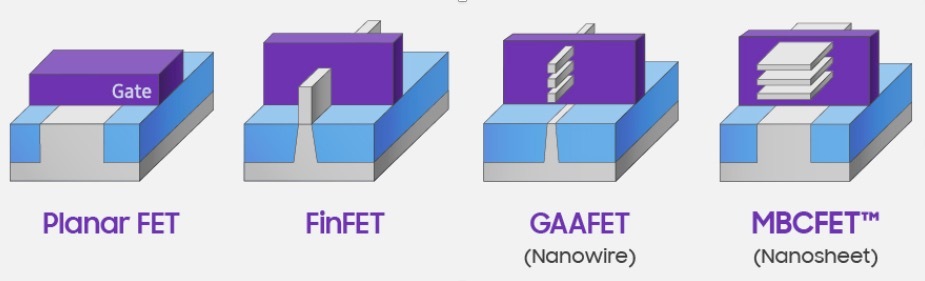
 In 2011, the goal for current leakage was 25% of the total power conusmption. But leakage can be as high as 50% for high perfromance chips. To provide better electrostatic control over the channel, the gate progress from the plannar design, to finFET, to GAAFET, to MBCFET.
 Source: Image extracted from [2]
As designs progress, the gate contact area with the channel increases. This provides better electrostatic control, which means the gate voltage more effectively controls whether the channel is on or off, thereby reducing leakage current when the transistor should be off.
Energy Efficiency in SRAM and DRAM
As transistor improvement decelerates, computer architects need to find other ways for improved energy efficiency. Given the energy budget in today’s system, it is easy today to design a microprocessor with many transistors that cannot all be turned on at the same time due to thermal constraints. This phenomenon has been called dark silicon. Some other ways to minimize energy consumption are to redesign the algorithm or kernel so that we can reduce the memory movement.
 Source: Image extracted from [1]
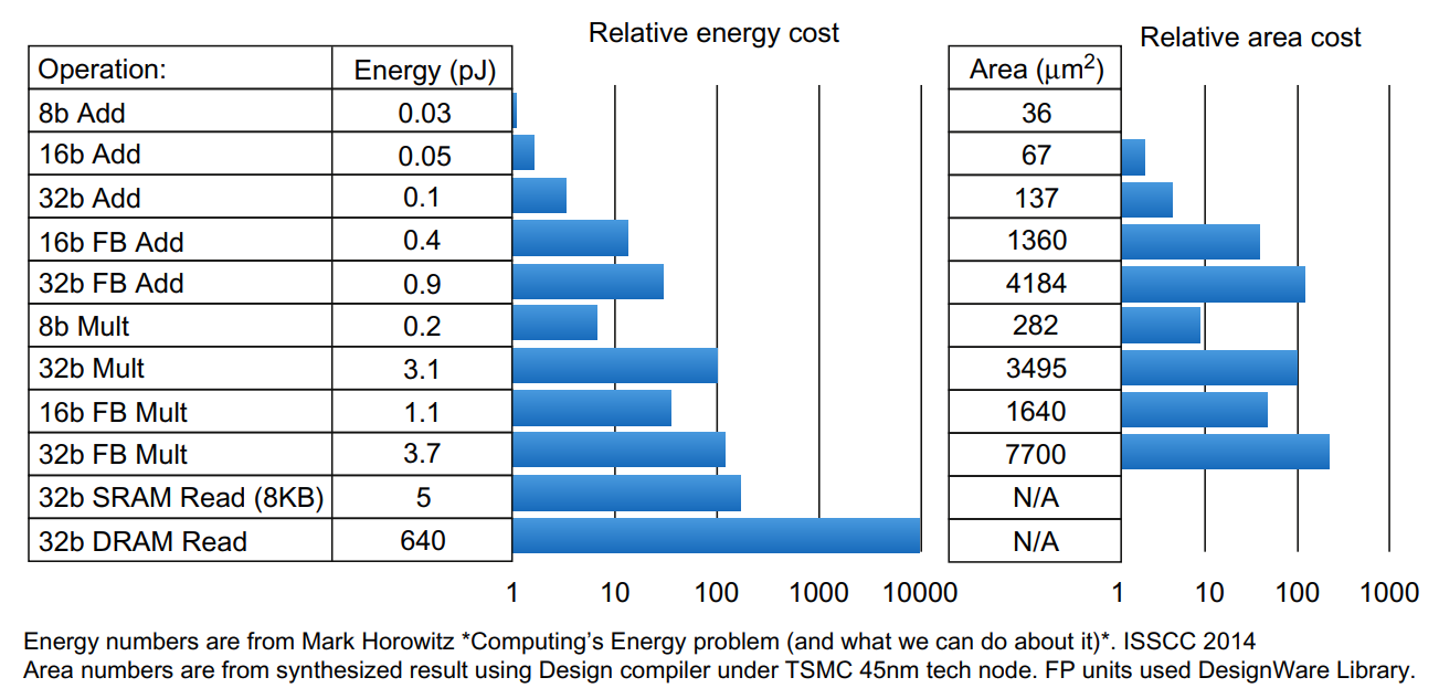
In real life, many applications are memory-bound due to the memory wall, where processor speed is much faster than memory speed. On top of that, we can see from the graph that SRAM and DRAM reads are much more power-consuming compared to Add and Mult operations. By reducing the data movement in the algorithm, we would be able to reduce the total power consumption very significantly.
All exponetial laws must come to an end
In summary, the breakdown of Dennard scaling (with its increased power density), the rise of static power leakage, thermal limits such as dark silicon, and wire delay limiting clock speeds have all contributed to the deceleration of Moore’s Law.
References
- Hennessy, John L., and David A. Patterson. Computer architecture: a quantitative approach. Elsevier, 2011.
- McLellan, Paul. “Samsung’s 3nm GAA Process.” Breakfast Bytes, Cadence Community, 21 May 2019, community.cadence.com/cadence_blogs_8/b/breakfast-bytes/posts/sam3nm.
- “P-N Junction.” DevXplained, 16 Nov. 2020, devxplained.eu/en/blog/p-n-junction.
- Kuphaldt, Tony R., et al. “The CMOS Transistor.” All About Circuits, www.allaboutcircuits.com/textbook/designing-analog-chips/analog-devices/the-cmos-transistor/.
- Θεοδώρου, Χριστόφορος Γ. Low-frequency noise in advanced CMOS/SOI nanoscale multi-gate devices and noise model development for circuit applications. Diss. Αριστοτέλειο Πανεπιστήμιο Θεσσαλονίκης, 2013.